 The semiconductors at the heart of high-tech applications are some of the most carefully scrutinized materials in the world. Even minuscule changes to their chemical compositions can lead to major improvement to their performance.
So it is rare for materials scientists to find something entirely surprising when analyzing these materials, but a team of researchers from the University of Utah and the University of Illinois have discovered the molecular equivalent of a Sasquatch.
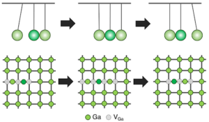
Called a “crowdion,” it is a long-hypothesized phenomenon within crystalline lattices featuring a rapid chain reaction of atoms crowded together repositioning, much like the suspended spheres in a Newton’s Cradle. The sequence of shifting bonds moves the location of an extra atom called an interstitial (or in this case, a vacancy — a spot in the lattice where an atom is missing) within the material.
The researchers observed this phenomenon in a variety of gallium oxide, a semiconductor eyed for its use in high-current, high-voltage applications. Controlling the formation of crowdions could make this extreme material even more durable. These moving defects might even be a useful feature of other semiconductors, with outside atoms riding these molecular conveyor belts from one part of the material to another.
Michael Scarpulla, a professor in the departments of Electrical & Computer Engineering and Materials Science & Engineering, collaborated with Elif Ertekin, an associate professor at the University of Illinois Urbana-Champaign, and Channyung Lee, a Ph.D student in her lab.
The findings were recently published in the journal Physical Review Materials.
Materials get their properties from the way their component atoms line up, which in turn determines how those atoms behave. Crystalline materials have their atoms tightly bonded in neat rows and columns; a piece of pure iron, for example, consists of iron atoms in a cubic lattice.
“The crowdion was first postulated in metals and silicon, when people were trying to figure out what would happen if a crystalline material had too many atoms in one spot — hence the ‘crowd’ in ‘crowdion,’” says Scarpulla. “It’s relatively easy to imagine in pure metals, but for semiconductors, the crowdion was thought to exist only under extreme conditions, if at all.”
Compound semiconductors have both metallic and nonmetallic elements in their lattices; the ionic oxygen in gallium oxide, for example, was thought to be too brittle to allow for the kind of sequential repositioning that more easily occurs in pure metals.
This quality is also one of the reasons the material is eyed for applications in power electronics: gallium oxide can withstand currents, voltages, and temperatures that would cause standard semiconductor materials like silicon to break down and fall apart. The researchers were therefore interested in getting a more comprehensive picture of the kinds of defects that can form in gallium oxide, with the ultimate goal of making it even more resistant to extreme conditions.
Given the difficulties of conducting experiments at the scale of individual atoms, simulations are invaluable to research conducted on such point defects in semiconductors. Lee, the study’s lead author, first made an exhaustive list of the kind of defects that could conceivably occur within gallium oxide’s crystalline structure, then painstakingly simulated the necessary conditions to see if they would actually form.
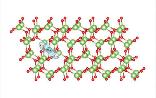
When Lee pulled back the virtual ball representing a gallium atom and let it collide with the rest of the lattice, the researchers were shocked to find that it set off a crowdion chain-reaction that synchronously moved multiple atoms, resulting in the vacancy defect moving deeper into the bulk of the simulated material.
Proving the existence of semiconductor crowdions gives the researchers a new direction when it comes to engineering these materials.
“It turns out that, because of these inch-worm-like defects, the atoms inside this material can move around really fast, and that can lead to the kind of breakdown we’re trying to prevent,” says Ertekin. “So if we want to make these materials stronger, we need to know more about why these crowdions are so mobile in the first place, and how we could engineer the material to limit that mobility”
Power electronics are not the only applications for gallium oxide, and there are many other semiconductor materials with the same basic structure that are likely to exhibit this phenomenon. More research into crowdions could unlock new abilities in entirely different fields.
“Sometimes, you want materials with ions that are easy to move,” says Lee. “We might be able to transport other atoms deeper into the material using those moving defects, and that could be useful for things like batteries and fuel cells.”
—###—
Investigation of Ga interstitial and vacancy diffusion in 𝛽−Ga2O3 via split defects: A direct approach via master diffusion equations
Channyung Lee, Michael A. Scarpulla, and Elif Ertekin
Phys. Rev. Materials
https://doi.org/10.1103/PhysRevMaterials.8.054603
The authors acknowledge the funding provided by the Air Force Office of Scientific Research under Award No. FA9550-21-0078. This work used PSC Bridges-2 at the Pittsburgh Supercomputing Center through allocation MAT220011 from the Advanced Cyberinfrastructure Coordination Ecosystem: Services & Support (ACCESS) program, which is supported by National Science Foundation Grants No. 2138259, No. 2138286, No. 2138307, No. 2137603, and No. 2138296.